XCV200E-6FG256C Device Overview and Functional Structure
Working with programmable hardware becomes easier when you understand how a device like the XCV200E-6FG256C operates inside a system. You can use it to create custom digital logic, manage signals, and connect different parts of electronic equipment through configurable circuits. Its programmable structure allows you to define logic behavior through configuration data rather than fixed wiring. With built-in memory, structured logic blocks, and many input and output connections, you get a flexible platform that supports control logic, signal handling, and communication functions within compact electronic designs.Catalog
XCV200E-6FG256C Overview
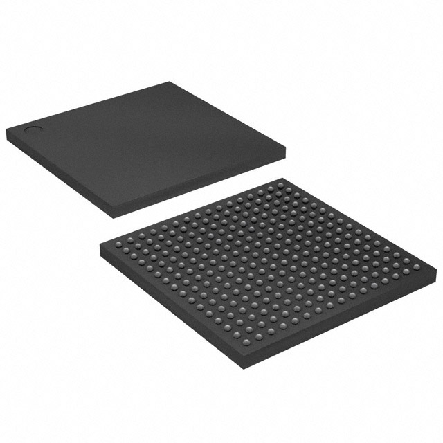
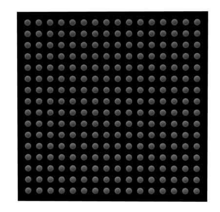
The XCV200E-6FG256C is a programmable logic device used to build custom digital functions inside electronic systems. It belongs to the Virtex-E FPGA family and integrates programmable logic cells, internal memory blocks, and routing paths that allow digital circuits to be defined through configuration data. The device provides 176 input and output connections and supports more than three hundred thousand logic gates for implementing control logic, data processing paths, and interface management. Operating from a 1.71 V to 1.89 V supply range, it uses a 256-ball FBGA package designed for surface mounted circuit boards in compact electronic equipment.
Looking for XCV200E-6FG256C? Contact us to check current stock, lead time, and pricing.
Banks of XCV200E-6FG256C
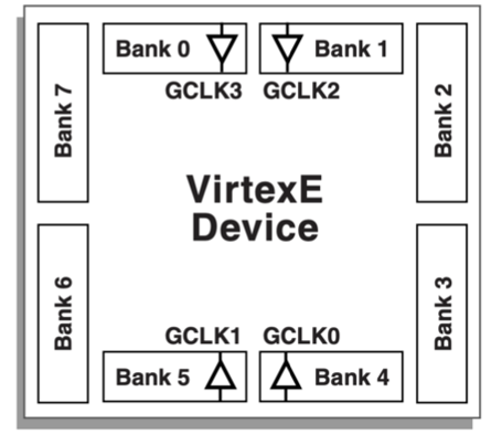
Input and output resources of the XCV200E-6FG256C are divided into eight separate banks arranged around the perimeter of the device to organize external signal connections. Each bank groups multiple Input Output Blocks that share common voltage and configuration settings for interface compatibility. Banks labeled 0 through 7 are positioned along the four sides of the device, forming the boundary between the internal programmable logic and the external package pins. Four global clock inputs labeled GCLK0, GCLK1, GCLK2, and GCLK3 are distributed across these banks to deliver clock signals into the internal routing network. This banked structure allows different signaling standards to operate in separate regions while maintaining consistent electrical behavior within each bank.
XCV200E-6FG256C CAD Model
XCV200E-6FG256C Symbol
XCV200E-6FG256C Footprint
XCV200E-6FG256C 3D Model
Features of XCV200E-6FG256C
Programmable Logic Fabric
The device contains a structured array of configurable logic blocks arranged across the chip to create digital circuits through programmable connections. Each block can implement combinational logic, small storage elements, and control functions, allowing designers to define custom digital behavior inside one component.
Embedded Block Memory
Integrated memory blocks provide internal storage that supports buffering, lookup tables, and temporary data handling during operation. These memory resources reduce the need for external memory devices and allow data processing tasks to occur directly inside the programmable logic structure.
High I O Connectivity
Up to 176 input and output connections are available to link the programmable logic with external components. These connections are arranged in organized banks, which allows the device to communicate with multiple system interfaces while maintaining consistent signal behavior across each bank.
Global Clock Distribution
Dedicated clock input paths distribute timing signals across the device through controlled routing channels. This arrangement keeps clock signals aligned across logic regions, helping sequential circuits operate in step with the system timing reference.
Internal Routing Network
An internal network of programmable interconnect lines links logic blocks, memory elements, and input output structures. These routing resources allow signals to travel between functional areas of the device and support flexible digital circuit layouts.
Surface Mount FBGA Package
The device uses a 256 ball fine pitch ball grid array package designed for surface mount assembly. This format supports compact circuit board layouts while providing the electrical connections required for logic signals, power distribution, and control lines.
Stable Supply Voltage Operation
Operation within a 1.71 V to 1.89 V supply range supports stable electrical behavior during system activity. This voltage range is suitable for programmable logic devices that integrate multiple functional blocks within a single silicon structure.
XCV200E-6FG256C Technical Specifications
| Product Attribute | Attribute Value |
| Manufacturer | AMD Xilinx |
| Voltage - Supply | 1.71V ~ 1.89V |
| Total RAM Bits | 114688 |
| Supplier Device Package | 256-FBGA (17x17) |
| Series | Virtex®-E |
| Package / Case | 256-BGA |
| Package | Tray |
| Operating Temperature | 0°C ~ 85°C (TJ) |
| Number of Logic Elements/Cells | 5292 |
| Number of LABs/CLBs | 1176 |
| Number of I/O | 176 |
| Number of Gates | 306393 |
| Mounting Type | Surface Mount |
| Base Product Number | XCV200E |
| RoHS Status | RoHS non-compliant |
| Moisture Sensitivity Level (MSL) | 3 (168 Hours) |
| REACH Status | REACH Unaffected |
| ECCN | 3A001A7B |
| HTSUS | 8542.39.0001 |
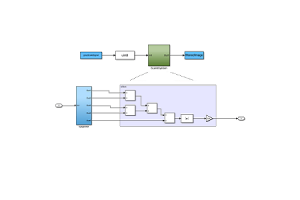
Architecture Overview of XCV200E-6FG256C
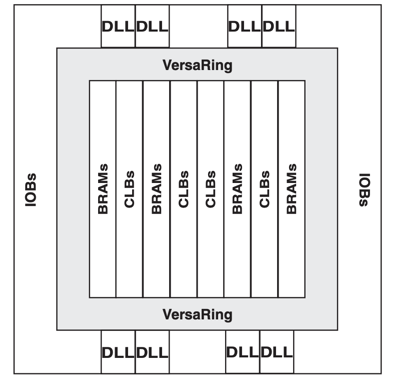
Central logic fabric arranged as vertical columns of Configurable Logic Blocks labeled CLBs forms the programmable core used to implement digital logic functions inside the XCV200E-6FG256C. Dedicated memory columns labeled BRAMs are distributed among the logic columns and provide embedded storage for data buffering and internal processing tasks. A routing structure labeled VersaRing surrounds the core region and provides additional signal paths that connect the logic array with the outer interface resources. Input and Output Blocks labeled IOBs line the outer perimeter of the device and connect the internal logic network to external pins of the package. Clock management resources labeled DLL are positioned along the edges of the architecture and support controlled distribution of clock signals across the programmable logic structure.
Input Output Block of XCV200E-6FG256C
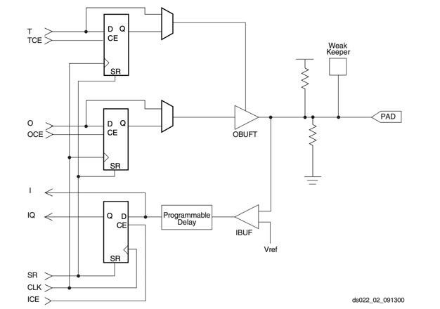
Internal input and output structure organized around a central pad connection defines how signals enter and leave the XCV200E-6FG256C device. Output data passes through a configurable flip flop stage with clock enable and set reset control before reaching a tri state output buffer labeled OBUFT that drives the external pad. Input signals arriving from the pad are routed through an input buffer labeled IBUF and can pass through a programmable delay stage before reaching internal logic registers. Additional control signals including clock, reset, and enable lines regulate data flow through the register stages. A weak keeper circuit connected to the pad maintains signal stability when the output driver is inactive, while reference voltage and termination elements support controlled signal levels for reliable interface operation.
Applications of XCV200E-6FG256C
Digital Signal Processing Platforms
Programmable logic resources allow the device to handle filtering, data transformation, and numeric processing tasks in signal processing systems. Its internal memory and configurable logic blocks support repeated arithmetic operations and structured data paths used in digital communication and measurement equipment.
Telecommunications Switching Equipment
Communication systems often require flexible data routing and protocol handling, and the device can be configured to manage these digital tasks. Programmable logic circuits allow switching behavior, packet handling, and control operations to be defined through configuration.
Industrial Control Systems
Industrial equipment frequently relies on programmable digital control structures to monitor inputs and drive outputs in automated processes. The device can coordinate sensors, timing signals, and control responses inside machines used in manufacturing and process management.
Embedded Computing Platforms
Embedded systems sometimes require dedicated hardware logic to manage timing, interface control, and specialized data handling. The device allows these digital circuits to be implemented inside a programmable logic structure without relying solely on software processing.
Data Acquisition Equipment
Measurement systems that collect signals from multiple sources can use programmable logic to organize sampling, buffering, and digital formatting of incoming data. Internal memory and routing resources help structure these data paths inside compact hardware platforms.
XCV200E-6FG256C Advantages and Disadvantages
Advantages
• Large programmable logic capacity supports complex digital circuits
• Integrated memory blocks allow internal data storage and buffering
• High number of input and output connections enables broad system integration
• Programmable architecture allows hardware behavior to be reconfigured
• Compact FBGA package supports dense circuit board layouts
Disadvantages
• Higher power usage than some smaller programmable logic devices
• Ball grid array package requires careful circuit board assembly
• Configuration requires external programming tools and design software
• Design complexity increases when implementing large digital systems
XCV200E-6FG256C Alternatives
| Part Number | Manufacturer | Key Features | Use Case/Notes |
| XCV200E-6FG456C | AMD | Virtex-E FPGA device containing about 5,292 logic cells and roughly 114 Kbits of embedded block RAM. It supports up to 176 I/O pins and operates with a core voltage near 1.8 V. The architecture uses configurable logic blocks and programmable routing to implement complex digital circuits. | Used in communication hardware, data processing equipment, and embedded computing systems where programmable logic can handle custom digital control and signal processing tasks. |
| XCV200E-6FG256I | AMD | Programmable FPGA from the Virtex-E series designed with configurable logic blocks, embedded memory, and flexible routing resources. It enables designers to create complex digital logic and interface circuits inside a single programmable device. | Often used in industrial control systems, digital instrumentation, and prototype hardware where programmable logic provides flexibility during design and testing. |
| XCV200E-6FG456I | AMD | High-capacity Virtex-E FPGA combining thousands of configurable logic cells with integrated block RAM and programmable routing networks. The architecture supports large digital designs and high I/O connectivity for complex hardware systems. | Suitable for telecommunications infrastructure, embedded system platforms, and advanced digital processing equipment that require flexible programmable hardware. |
About AMD Xilinx
AMD Xilinx develops programmable logic devices used in electronic systems that require configurable digital hardware. The company began in 1984 and introduced the first commercially available field programmable gate array, establishing a widely used approach to hardware design based on programmable logic. Its product portfolio includes FPGA devices, adaptive computing platforms, and system integration tools used in communication systems, data centers, industrial equipment, and embedded electronics. The technology allows digital circuits to be configured through software design tools, enabling flexible hardware development for a wide range of electronic applications.
Conclusion
The XCV200E-6FG256C is a programmable logic device that allows you to build custom digital circuits inside a single component. Its architecture combines configurable logic blocks, internal memory, and routing paths that work together to form flexible digital systems. Organized input and output banks help connect the device with external components while maintaining stable signal behavior. Clock distribution and programmable interconnect structures allow signals to move across the chip in a structured way. With these capabilities, you can implement control logic, data processing paths, and communication interfaces within compact electronic designs. Understanding its architecture, features, and applications helps you see how programmable logic devices fit into modern electronic systems.
Datasheet PDF
XCV200E-6FG256C Datasheet:
O nas
ALLELCO LIMITED
Preberi več
Hitro povpraševanje
Prosimo, pošljite poizvedbo, takoj bomo odgovorili.
Pogosto zastavljena vprašanja [FAQ]
1. What type of device is the XCV200E-6FG256C?
The XCV200E-6FG256C is a field programmable gate array, often called an FPGA. It allows you to create custom digital circuits using programmable logic blocks and internal routing resources.
2. How many input and output connections does the XCV200E-6FG256C have?
The device provides up to 176 input and output connections. These connections allow the FPGA to communicate with external components such as sensors, processors, or communication interfaces.
3. What is the main function of the internal logic blocks in the XCV200E-6FG256C?
Configurable logic blocks inside the device implement digital functions such as combinational logic, storage elements, and control circuits. These blocks form the core programmable structure of the FPGA.
4. What role do the I/O banks play in the XCV200E-6FG256C?
I/O banks organize the device’s external connections into groups around the perimeter of the chip. Each bank supports multiple input and output blocks that connect internal logic to the package pins.
5. Where can the XCV200E-6FG256C be used?
The device can be used in signal processing systems, telecommunications equipment, industrial control systems, embedded computing platforms, and data acquisition hardware where programmable digital logic is needed.

392 Priročnik za velikost, uporabo in zamenjavo baterije
na 2026/03/16
Praktični vodnik za čip EPF10K30AFC484-1 FPGA
na 2026/03/13
Priljubljene objave
-
Kompleksni nastavitveni računalniki: Kako so spremenili računalništvo?
na 8000/04/18 147776
-

USB-C pinout in funkcije
na 2000/04/18 112022
-
Uporaba Xilinx Unified Simulacijske primitive: Obsežen vodnik za oblikovanje in simulacijo FPGA
na 1600/04/18 111351
-
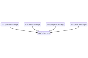
Napajalne napetosti v elektroniki: pomen VCC, VDD, VEE, VSS in GND
na 0400/04/18 83777
-
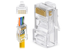
Vodnik priključkov RJ45: pinout, ožičenje, vrste kablov in uporabe
na 1970/01/1 79575
-

Ultimate Guide za žičnice barvnih kod v sodobnih električnih sistemih
Način, kako naši električni sistemi uporabljajo barve, ni samo za videz.Vsaka barva žice zdaj označuje določeno funkcijo, kar olajša pravilno prepoznavanje in ravnanje z električnimi komponentami m...na 1970/01/1 66964
-

Vodnik za čiščenje ventila: funkcija, simptomi, testiranje in zamenjava za optimalno delovanje motorja
Čistilni ventil je ključni del sistema avtomobila, ki pomaga ohranjati čist zrak z upravljanjem hlapov goriva, preden lahko pobegnejo v ozračje.To ne samo pomaga okolju z zmanjšanjem onesnaževanja,...na 1970/01/1 63104
-

Faktor kakovosti (q): enačbe in aplikacije
Faktor kakovosti ali "Q" je pomemben pri preverjanju, kako dobro induktorji in resonatorji delujejo v elektronskih sistemih, ki uporabljajo radijske frekvence (RF).'Q' meri, kako dobro vezje minimi...na 1970/01/1 63041
-
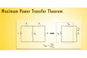
Doseganje največjih zmogljivosti z največjim teoremom o prenosu energije
Teorem največjega prenosa moči pojasnjuje, kako energija iz vira, na primer baterija ali generator, teče v povezano obremenitev.Prikaže natančen pogoj, kjer obremenitev prejme največ moči.Ta članek...na 1970/01/1 54097
-

A23 Specifikacije baterije in združljivost
Akumulator A23 je majhna baterija v obliki valja z visoko napetostjo.Imenovan tudi 23A, 23AE ali MN21, deluje pri 12 voltih in veliko višji od baterij AA ali AAA.Njegova posebna zasnova je...na 1970/01/1 52189
Vroča številka dela
-
AFE7070IRGZR
Texas Instruments
IC DAC 14BIT V-OUT 48VQFN
NTD5867NL-1G
onsemi
MOSFET N-CH 60V 20A IPAK
ADS1294IPAGR
Texas Instruments
IC AFE 4 CHAN 24BIT 64TQFP
Z84C1510FEG
Zilog
IC MPU Z80 10MHZ 100QFP
MCP619T-I/SL
Microchip Technology
IC CMOS 4 CIRCUIT 14SOIC
IS43R16800E-5TL
ISSI, Integrated Silicon Solution Inc
IC DRAM 128MBIT PAR 66TSOP II
5745171-5
TE Connectivity AMP Connectors
CONN BACKSHELL 9POS 180DEG SHLD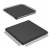
CY7C1460SV33-200AXC
Infineon Technologies
IC SRAM 36MBIT 200MHZ 100TQFP
83PR226BKI-01LF
Renesas Electronics America Inc
IC CLK/FREQ SYNTH 10VFQFPN
TCS37013
ams OSRAM
SENSOR AMBIENT LIGHT
TLK2226ZEA
Texas Instruments
IC TRANSCEIVER FULL 2/2 196BGA
TLV2402IDRG4
Texas Instruments
IC OPAMP GP 2 CIRCUIT 8SOIC
EMZA350ARA101MF80G
United Chemi-Con
CAP ALUM 100UF 20% 35V SMD
OR2C15A4S240-DB
Lattice Semiconductor Corporation
FPGA, 400 CLBS, 19200 GATES
2SC2462LCTL-E
Renesas Electronics America Inc
TRANS NPN 40V 0.1A 3MPAK
06035A180FA12A
KYOCERA AVX
CAP CER 18PF 50V C0G/NP0 0603
MIC5203-3.3YM5-TR
Microchip Technology
IC REG LINEAR 3.3V 80MA SOT23-5
AD9691BCPZ-1250
Analog Devices Inc.
IC ADC 14BIT PIPELINED 88LFCSP -
AP7340D-12FS4-7
Diodes Incorporated
IC REG LINEAR 1.2V 150MA 4DFN
SZT1010T1G
onsemi
TRANS SOT223
CPC1465DTR
IXYS Integrated Circuits Division
IC TELECOM INTERFACE 16SOIC
TAC-10-683-D
Cosel USA, Inc.
LINE FILTER 500VAC 10A DIN RAIL
GRM1555C1H470JA01D
Murata Electronics
CAP CER 47PF 50V C0G/NP0 0402
FCPF4300N80Z
onsemi
MOSFET N-CH 800V 1.6A TO220F
74VHCU04SJ
Fairchild Semiconductor
IC INVERTER 6CH 1-INP 14SOP
R1LV5256ESP-7SR#S0
Renesas Electronics America Inc
IC SRAM 256KBIT PARALLEL 28SOP
TL061CD
STMicroelectronics
IC OPAMP JFET 1 CIRCUIT 8SOIC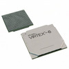
XC5VLX330-1FF1760I
AMD
IC FPGA 1200 I/O 1760FCBGA
AQV210EAZ
Panasonic Electric Works
SSR RELAY SPST-NO 130MA 0-350V
TCAN1042HD
Texas Instruments
IC TRANSCEIVER 1/1 8SOIC
CD22402E
Harris Corporation
SYNC GENERATOR FOR TV
WRF0505S-1WR2
Mornsun America, LLC
ISOLATED MODULE DC DC CONVERTER
MK2069-04GILFTR
Renesas Electronics America Inc
IC CLOCK SYNCHRONIZER 56TSSOP
VLCF5024T-4R7N1R3-2
TDK Corporation
FIXED IND 4.7UH 1.33A 44MOHM SMD
AD7809BST
Analog Devices Inc.
IC DAC 10BIT OCTAL PARALL 44TQFP
FH42-7S-0.3SHW(10)
Hirose Electric Co Ltd
CONN FFC FPC 0.3MM SMD -

CPT300100D
Microsemi Corporation
DIODE MODULE 100V TO244AB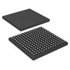
PI7C9X2G608GPBNJE
Diodes Incorporated
IC INTFACE SPECIALIZED 196LBGA
53916-0208
Affinity Medical Technologies - a Molex company
CONN PLUG 20POS 4MM SMD .5MM
AMS1117-1.2
UMW
SOT223-3L LINEAR VOLTAGE REGULAT
08055A2R0BAT2A
AVX Corporation
CAP CER 2PF 50V NP0 0805
BU94604KV-E2
Rohm Semiconductor
IC DECODER AAC WMA MP3 64-VQFP
MAX1489EESD
Analog Devices Inc./Maxim Integrated
IC RECEIVER 0/4 14SOIC
ATMXT540E-CCUR
Atmel
IC SENSOR MAXTOUCH
FTBVP5SH50
Fairchild Semiconductor
FTBVP5SH50
PIC12F1501-I/SN
Microchip Technology
IC MCU 8BIT 1.75KB FLASH 8SOIC
AS1323-BTTT-33
ams OSRAM
IC REG BOOST 3.3V 1A TSOT23-5
CL05C090DB5NNNC
Samsung Electro-Mechanics
CAP CER 9PF 50V C0G/NP0 0402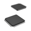
EX256-TQ100
Microchip Technology
IC FPGA 81 I/O 100TQFP
GRM31CR71E475KA88K
Murata Electronics
CAP CER 4.7UF 25V X7R 1206
BD5225FVE-TR
Rohm Semiconductor
IC SUPERVISOR 1 CHANNEL 5VSOF
AT93C66B-MEHM-T
Microchip Technology
IC EEPROM 4KBIT 3-WIRE 8XDFN
DR74-3R3-R
Eaton - Electronics Division
FIXED IND 3.3UH 3.94A 18.3 MOHM
NCV8114BSN280T1G
onsemi
IC REG LINEAR 2.8V 300MA 5TSOP